[GPU] Tensor Core
1. tensor core 란
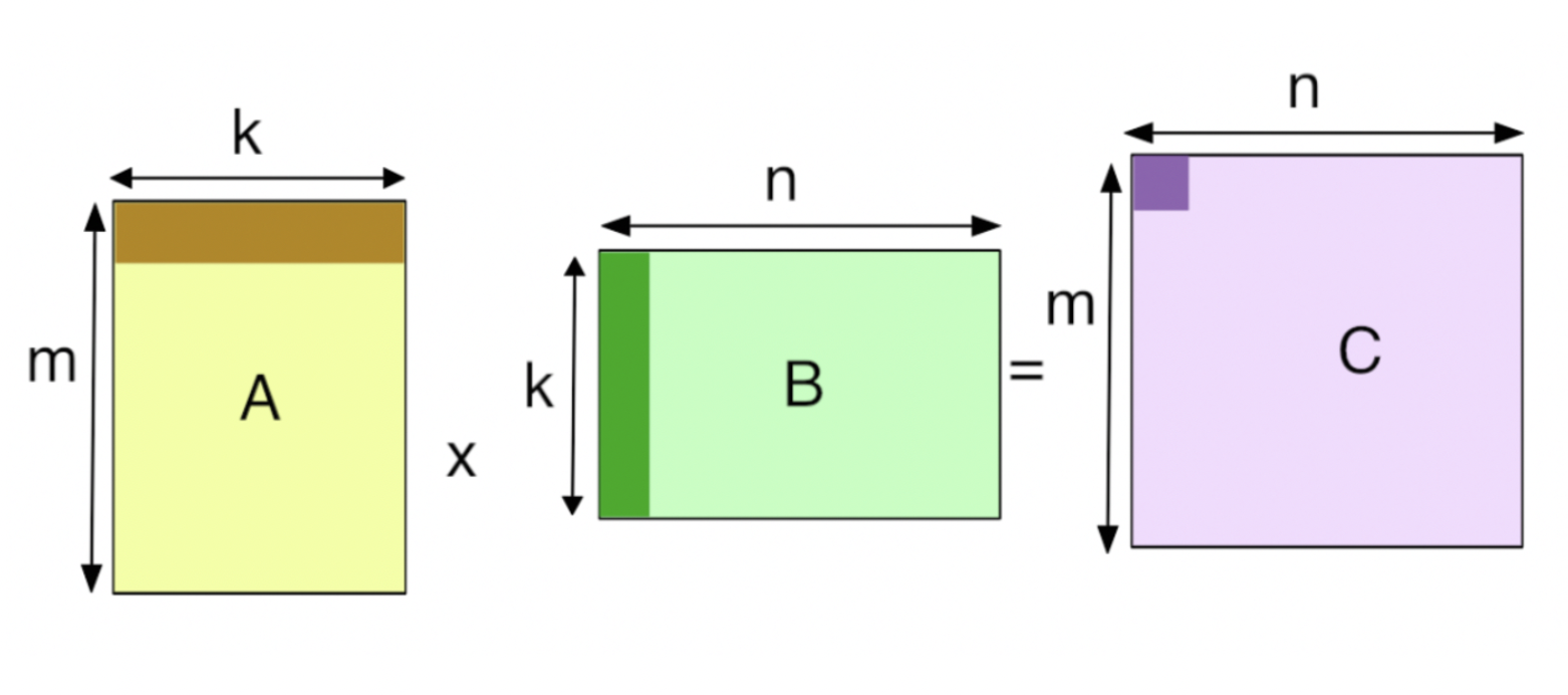
행렬 곱셈과 덧셈을 수행하는 함수 단위입니다. 이 연산을 mma라고 표현하기도 하는데 FMA연산과 같습니다.
참고로 텐서(tensor)는 행렬을 의미한다. 딥러닝은 행렬 연산으로 이루어지므로 구글의 딥러닝 라이브러리 또한 이름이 텐서플로(tensorflow)입니다.
Unlike Pascal GPUs, which could not execute FP32 and INT32 instructions simultaneously, the Volta GV100 SM includes separate FP32 and INT32 cores, allowing simultaneous execution of FP32 and INT32 operations at full throughput, while also increasing instruction issue throughput.
Dependent instruction issue latency is also reduced for core FMA (Fused Multiply-Add) math operations, requiring only four clock cycles on Volta, compared to six cycles on Pascal.

그림에서, 텐서 코어는 행렬 곱을 수행하고 그 결과를 C에 축적합니다.(FMA) 이때 D의 요소 16개는 동시에 계산됩니다. 하나의 텐서코어는 64개의 mma연산을 한 사이클에 수행합니다. 즉, 4x4 행렬곱의 결과를 한 사이클에 계산할 수 있는 것입니다.
두 개의 행렬 곱을 한 값이 FP32이 입니다. 결과 비트가 입력 비트와 다른 것을 두고 mixed precision이라고 합니다.

이런 연산 과정을 위한 유닛을 왜 만들었을까요?
고성능 컴퓨팅에서 이 연산이 자주 쓰이기 때문입니다.
이건 GEMM 연산,
텐서코어 연산을 위해, 다단계 파이프라인이 필요할 것이라고 한다. multistage pipeline이 무엇인지 알아보았다.
파이프라인은 한 데이터의 출력이 다음에 입력으로 이어지는 구조이고
C에 축적되는 과정에서 다단계 파이프라인 구조를 통해 회색 큐브로 그려지는 AXB 연산 값들을 더해서 담지 않을까.

한 set에서 A는 4x4 벡터, B는 4x8 벡터를 데려다 계산합니다. 이 4개의 셋은 한 사이클에 연산이 끝나야 하고, 스레드 그룹0는 D의 4x8

D의 한 스레드 그룹(4x8)은 4 번의 스텝으로 계산이 됩니다.

텐서 코어 관련 논문에서 연산 수행 과정을 step 이라고 총칭하다가 Turing에서는 그렇지 않다고 합니다. 연산 수행 과정은 어떻게 달라졌는지 이해가 필요합니다.
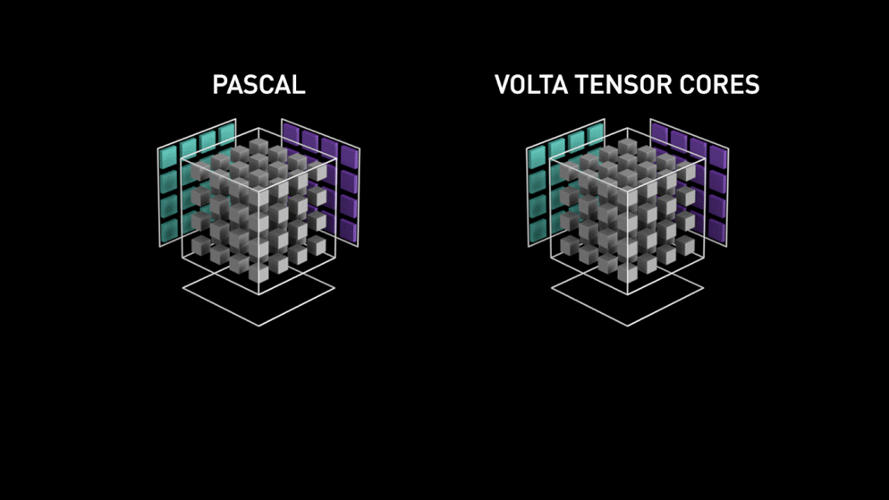
왼쪽은 행렬 내의 각 요소를 개별적으로 계산하는 파스칼 아키텍처이고, 오른쪽은 전체 작업을 한 번에 끝내는 볼타 아키텍처입니다.
애니메이션에서 텐서코어는 파스칼의 SM이 행렬 곱을 한 번 하는 시간에 12개의 행렬 곱을 합니다.
파스칼 아키텍처의 매트릭스 mul 연산 과정이 이해가 가지 않습니다.
파란 행렬은 왜 한 칸 씩 참고하고 보라색 행렬은 한 줄씩 참고하나요?
그리고 초록색 한 칸이 만들어지는 게 이해가 안 갑니다.
--> 이건 홍보용 이미지이므로 구체적인 구조 이해에 참고가 될 수 없다.

각 텐서코어는 한 클럭에서 64개의 연산을 수행합니다. 출력한 행렬의 한 요소(element)를 계산하는 데에 4개의 FMA 연산이 필요하고 총 4x4개의 요소가 있기 때문입니다.
once again this is a diagram from one of nvdia's blocks which shows how a small slice of the computation is done. note that this is computing a single fuse multiply add. also note here that there are three inputs to the adder. one from the multiplication one from the F32 input or matrix C in the previous slide and one from additional products.
the first thing to note here is that binary arithmetic which is what the floating point adder is doing can only be done pairwise. this means that essentially these three additions need to be made up of two smaller additions or they have to use a more complicated piece of hardware called a compressor.
the next thing to note is that floating point is complicated. because of denormalization and renormalization steps required. luckily the FP numbers do not need to be denormalized before going into the multiplier but they do need to be realigned afterwards and after every addition. and finally, notice the output and addition is a 32-bit FP number but the two inputs to the multiplication are 16-bit FP numbers. this is most likely due to the reason mentioned in a previous video that multiplication of two 32-bit numbers would result in a maximum of a 64-bit result. and similarly two 16-bit numbers result in a 32-bit result. a small footnote here is that a 16-bit FP number doesn't actually occupy 16 bits for the mantissa. however the concept still applies.

the block diagram on the screen is a processor block also known as a partition. there are four processor blocks within a single streaming multiprocessor or SM. each processor block is capable of executing its own instructions however the processor block is only capable of issuing a single instruction to the entire block. this is done via the warp and dispatch units.
note that this is an implementation of SIMD. so you can for example multiply to 16 elements arrays together in a single instruction by using all 16 floating-point 32 units.
note that all of these units are executing the same instruction or a single thread is scheduled on a single FP 32 unit. for the note, that because of this architecture, branching instructions at the thread level are inefficient and a final note is that FP 32 units are what NVIDIA calls CUDA cores where there are 16 per processor block which cannot execute individual instructions.
looking at the block diagram of one of the 4 processor blocks within a single Volta SM. we can see that there are two tensor cores. and that they are massive. each tensor core is divided into a series of 64 blocks spread out in a four by 16 grid. most likely, a vertical axis of 16 blocks represents the resultant matrix elements which since we are dealing with a 4 by 4 matrices that total 16 then horizontally, we have the four fused multiply add units.
the next thing to consider are the stated latencies and throughput. according to the Volta architecture white paper, one of the FP 32 fused multiply add units(FMA) as a latency of four clock cycles while the pascal units had latency of six cycles. additionally, one academic paper cited the white paper claiming that the tensor cores have a throughput of one operation per cycle. a throughput of one per cycle should be possible if done correctly. note that while it's possible to make use of the main FP 32 FMA units for these tensor core operations it's unlikely that they are helping since the required signal routing between the two sides would be a nightmare.
쿠다의 라이브러리 가운데 cuBLAS와 cuDNN이 텐서 코어를 지원합니다. 텐서 코어의 동작 방식을 알기 위해서는 해당 라이브러리를 사용하는 애플리케이션을 돌려보면 알 수 있습니다.

turing adds INT8 and INT4 precision modes -> it can tolerate quantization
2. HBM2 MEMORY ARCHITECTURE

HBM2 offers three times (3x) the memory bandwidth of the Maxwell GM200 GPU.
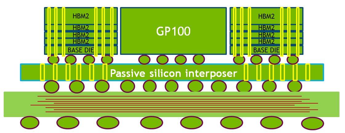
The HBM2 stack in the upper left is built out of five die-- a base die and 4 memory die above it. The top memory die layer is very thick. When assembled, the top die and GPU are ground to the same height to present a coplanar surface for a heat sink.
As shown in the GP100 full-chip block diagram (Figure 7), the GP100 GPU connects to four HBM2 DRAM stacks. Two 512-bit memory controllers connect to each HBM2 stack for an effective 4096-bit-wide HBM2 memory interface. Initially, Tesla P100 accelerators will ship with four 4-die HBM2 stacks, for a total of 16 GB of HBM2 memory.
HBM2 offers higher memory capacity and memory bandwidth. HBM2 supports four or eight DRAM dies per stack, while HBM1 only supports four DRAM dies per stack.
HBM2 memory is composed of providing substantial power and area savings compared to traditional GDDR5 memory designs, thus permitting more GPUs to be installed in servers.
Because HBM2 memory is stacked memory and is located on the same physical package as the GPU, it provides considerable space savings compared to traditional GDDR5, which allows us to build denser GPU servers more easily than ever before.
HBM2 in Tesla V100 uses four memory dies per HBM2 stack, and four stacks, with a maximum of 16 GB of GPU memory.
The HBM2 memory delivers 900 GB/sec of peak memory bandwidth across the four stacks.
The Tesla V100 HBM2 memory subsystem supports Single-Error Correcting Double-Error Detecting (SECDED) Error Correction Code (ECC) to protect data.

Another benefit of HBM2 memory is native support for error correcting code (ECC) functionality. ECC provides higher reliability for compute applications that are sensitive to data corruption. It is especially important in large-scale cluster computing environments where GPUs process very large datasets and/or run applications for extended periods.
ECC technology detects and corrects single-bit soft errors before they affect the system. In comparison, GDDR5 does not provide internal ECC protection of the contents of memory and is limited to error detection of the GDDR5 bus only. Errors in the memory controller or the DRAM itself are not detected.
GK110 Kepler GPUs offered ECC protection for GDDR5 by allocating some of the available memory for explicit ECC storage. 6.25% of the overall GDDR5 is reserved for ECC bits. In the case of a 12 GB Tesla K40 (for example), 750 MB of its total memory was reserved for ECC operation, resulting in 11.25 GB (out of 12 GB) of available memory with ECC turned on for Tesla K40. Also, accessing ECC bits caused a decrease in memory bandwidth of 12-15% on typical workloads, compared to the non-ECC case. Since HBM2 supports ECC natively, Tesla P100 does not suffer from the capacity overhead, and ECC can be active at all times without a bandwidth penalty. Like the GK110 GPU, the GP100 GPU’s register files, shared memories, L1 cache, L2 cache, and the Tesla P100 accelerator’s HBM2 DRAM are protected by a Single‐ Error Correct Double‐Error Detect (SECDED) ECC code.
3. UNIFIED MEMORY AND ADDRESS TRANSLATION SERVICES
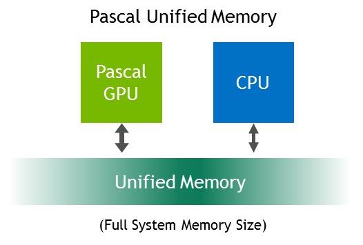
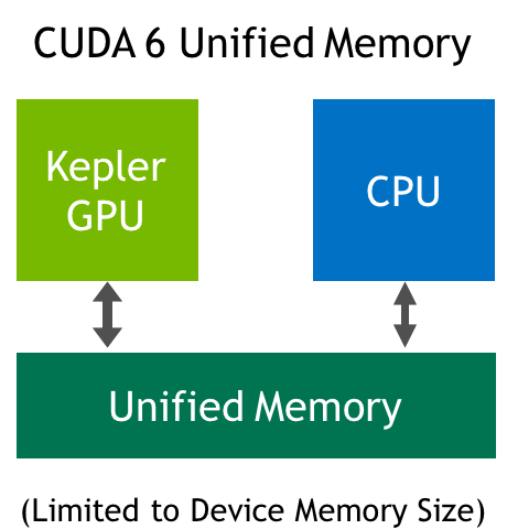
GP100 extends GPU addressing capabilities to enable 49-bit virtual addressing. This is large enough to cover the 48-bit virtual address spaces of modern CPUs, as well as the GPU's own memory. This allows GP100 Unified Memory programs to access the full address spaces of all CPUs and GPUs in the system as a single virtual address space, unlimited by the physical memory size of any one processor (upper one).
A limited form of Unified Memory was introduced with CUDA 6 in our Kepler and Maxwell GPUs, and it was improved with hardware page faulting and a larger address space in the Pascal GP100 GPU.
Programmers no longer need to worry about managing data sharing between GPU and CPU virtual memory systems.
Unified Memory in Pascal GP100 provided transparent migration of data between the full virtual address spaces of both the GPU and CPU.
4. Volta architecture - thread scheduling
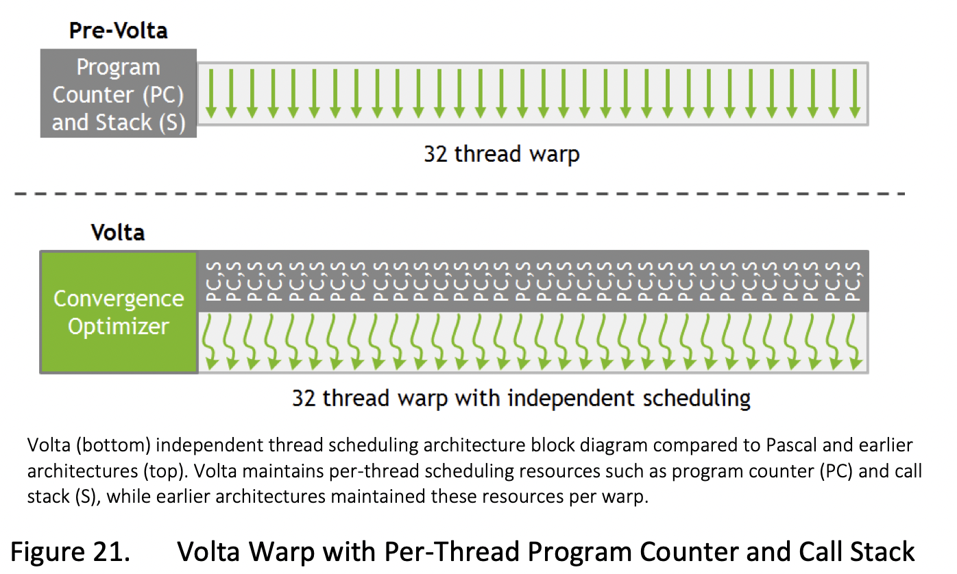
Volta transforms this picture by enabling equal concurrency between all threads, regardless of warp.
워프와 관련없이 스레드 간의 concorrency
To maximize parallel efficiency, Volta includes a schedule optimizer which determines how to group active threads from the same warp together into SIMT units.
This retains the high throughput of SIMT execution as in prior NVIDIA GPUs, but with much more flexibility: threads can now diverge and reconverge at sub-warp granularity, while the convergence optimizer in Volta will still group together threads which are executing the same code and run them in parallel for maximum efficiency
# turing architecture white paper
feature)
1) new SM
Turing introduces a new processor architecture, the Turing SM, that delivers a dramatic boost in shading efficiency, achieving 50% improvement in delivered performance per CUDA Core compared to the Pascal generation.
- First, the Turing SM adds a new independent integer datapath that can execute instructions concurrently with the floating-point math datapath. In previous generations, executing these instructions would have blocked floating-point instructions from issuing.
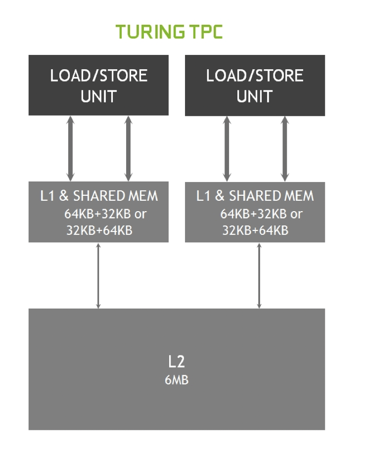
- Second, the SM memory path has been redesigned to unify shared memory, texture caching, and memory load caching into one unit.
Turing SM is partitioned into four processing blocks each with 16 FP32 Cores, 16 INT32 Cores, two Tensor Cores, one warp scheduler, and one dispatch unit.
Each block includes a new L0 instruction cache and a 64 KB register file. The four processing blocks share a combined 96 KB L1 data cache/shared memory.
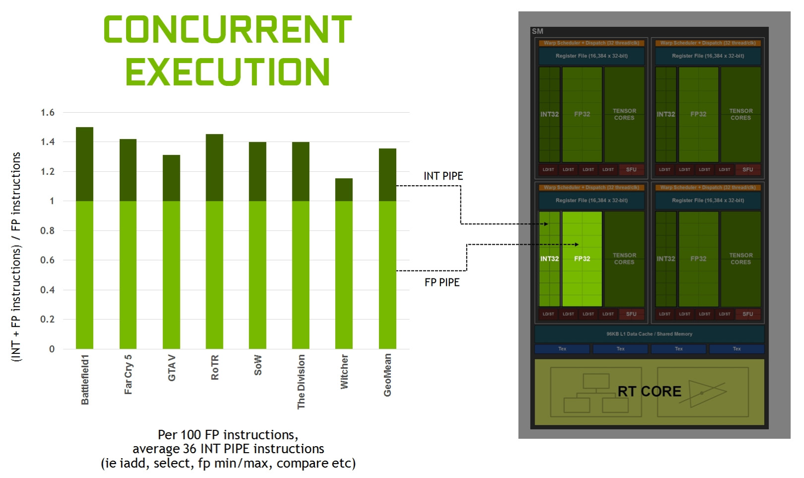
Figure 5 shows that the mix of integer pipe versus floating point instructions varies, but across several modern applications, we typically see about 36 additional integer pipe instructions for every 100 floating point instructions. Moving these instructions to a separate pipe translates to an effective 36% additional throughput possible for floating point.
Turing’s SM also introduces a new unified architecture for shared memory, L1, and texture caching. This unified design allows the L1 cache to leverage resources, increasing its hit bandwidth by 2x per TPC compared to Pascal, and allows it to be reconfigured to grow larger when shared memory allocations are not using all the shared memory capacity.
Combining the L1 data cache with the shared memory reduces latency and provides higher bandwidth than the L1 cache implementation used previously in Pascal GPUs.
2) tensor core
Turing GPUs include a new version of the Tensor Core design that has been enhanced for inferencing. Turing Tensor Cores add new INT8 and INT4 precision modes for inferencing workloads that can tolerate quantization and don’t require FP16 precision.
A TU102 GPU contains 576 Tensor Cores: eight per SM and two per each processing block within an SM. Each Tensor Core can perform up to 64 floating point fused multiply-add (FMA) operations per clock using FP16 inputs. Eight Tensor Cores in an SM perform a total of 512 FP16 multiply and accumulate operations per clock, or 1024 total FP operations per clock. The new INT8 precision mode works at double this rate, or 2048 integer operations per clock.
3) memory architecture
Turing improves main memory, cache memory, and compression architectures to increase memory bandwidth and reduce access latency.
NVIDIA GPUs utilize several lossless memory compression techniques to reduce memory bandwidth demands as data is written out to frame buffer memory.